RF DESIGN
RF front-ends, done right the first time.
From schematic to shielded enclosure — analog, mixed-signal and wideband design that passes compliance and performs in the real world.

From schematic to shielded enclosure — analog, mixed-signal and wideband design that passes compliance and performs in the real world.
RF engineering is the invisible layer under GPS, cellular, Wi-Fi, Bluetooth, IoT and satellite links. Getting it right means a radio that works in a crowded spectrum at the edges of environmental tolerance — on a tight BOM and thermal envelope. Getting it wrong shows up as dropped calls, failed compliance, truck rolls and spec recalls. We think about these four pressures on every program.
As 5G FR1/FR2, Wi-Fi 7 and LPWAN stack into the same boards, inter-stage isolation and adjacent-channel rejection become the critical constraints — not raw sensitivity. Link budgets are built backwards from the interferer profile.
A modern radio is a chain of power amplifiers, low-noise amplifiers, filters, mixers, synthesizers, switches and antennas — sometimes on a module, sometimes as discrete SMT, always tied together by a PCB stack-up that we co-design with the silicon choice.
GaN for high-efficiency PA. GaAs for linearity at millimeter-wave. SiGe BiCMOS for cost-sensitive IF paths. CMOS where integration wins. The material choice upstream dictates the thermal, matching and compliance work downstream — and we size it in week one, not week twenty.
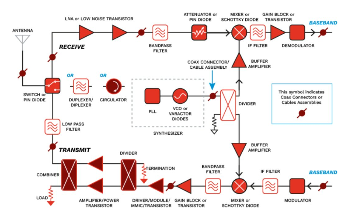
Every radio we ship — handset, base-station, IoT module or SATCOM modem — resolves into some variation of this block diagram. The receive path pulls a microvolt-level signal out of the antenna, rejects the neighbors, down-converts to IF and demodulates. The transmit path does the reverse, up-converting baseband through a driver and power amplifier back to the antenna. Each block is a trade-off — and trade-offs are where experience earns its money.
Our senior RF engineers have shipped designs across these bands. “Shipping” means: in production, passing compliance, reviewed peer-to-peer.
Every RF block we ship is validated in simulation before it touches a VNA. That’s how we hit first-pass compliance on programs where the schedule doesn’t allow a second spin.
Scope sized to what you actually need. Pricing and timeline fixed before we start.
Full RF module from block diagram to shipping product: schematic, layout, mechanical, firmware, test fixture, compliance report, documentation.
Learn more →Senior RF engineer audits your schematic, layout, or test setup. Written report + risk-ranked action list. Typical duration 3-5 days.
Learn more →DFM review, test fixture design, calibration procedures, factory documentation — moving a validated prototype to volume production.
Learn more →Each phase has a hard deliverable your team can review. No “trust us, it’s progressing” updates — you see the artifacts at every gate.
Block diagram, link budget, part-selection trade-off. 1-2 weeks.
Full schematic review, DRC clean, part-level SI simulation. 3-4 weeks.
Multi-layer PCB with controlled impedance, SI/PI sim, thermal. 3-5 weeks.
Bring-up board + test fixture, bench characterization. 4-6 weeks.
Pre-compliance in-house, formal compliance with partner lab. 4-8 weeks.
Not just slides. Real, audit-ready deliverables that your next vendor (or your internal team) can pick up without our involvement.
Schematic (source), layout (ODB++), BOM, AVL, mechanical CAD, fabrication drawing.
SI/PI simulation reports, lab test data, link-budget spreadsheet, measurement traces.
Pre-compliance test report, DoC draft, risk register, recommended production test plan.
Talk to our Singapore engineering team about your RF, FPGA/DSP, or AI inference project. We'll help you pick the right silicon and ship on time.